Circuit topology is the way power devices and electromagnetic components are connected in a circuit, and magnetic component design, closed-loop compensation circuit design, and all other circuit component designs depend on topology. The most basic topologies are Buck (buck), Boost (boost) and Buck/Boost (boost/buck), single-ended flyback (isolated flyback), forward, push-pull, half-bridge and full-bridge. Changer. There are about 14 common topologies of switching power supplies, each with its own characteristics and applicable situations. The selection principle depends on whether it is high power or low power, high voltage output or low voltage output, and whether it requires as few components as possible. To choose a topology appropriately, it is important to be familiar with the advantages, disadvantages, and applicability of various topologies. The wrong choice can doom a power supply design to failure from the start.
In this article, we will provide an in-depth look at different aspects of buck, boost, and buck-boost topologies. And a summary of 20 basic topologies of switching power supplies.
Table of Contents
Buck Converter
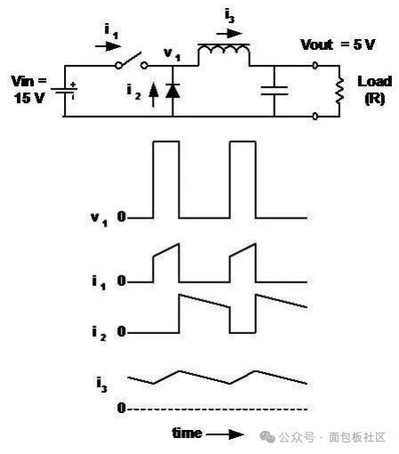
Figure 1 is a schematic diagram of a nonsynchronous buck converter. A buck converter reduces its input voltage to a lower output voltage. When switch Q1 turns on, energy is transferred to the output.
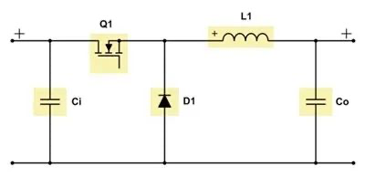
Figure 1: Non-synchronous buck converter schematic
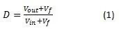
Equation 1 calculates the duty cycle:
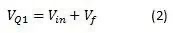
Equation 2 calculates maximum metal oxide semiconductor field effect transistor (MOSFET) stress:
Equation 3 gives the maximum diode stress:
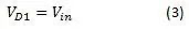
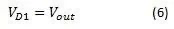
Where Vin is the input voltage, Vout is the output voltage, and Vf is the diode forward voltage.
The greater the difference between the input voltage and the output voltage, the more efficient a buck converter is compared to a linear regulator or a low dropout regulator (LDO).
Although the buck converter has pulsed current at the input, the output current is continuous due to the inductor-capacitor (LC) filter located at the output of the converter. As a result, the voltage ripple reflected to the input will be larger compared to the ripple at the output.
For buck converters with small duty cycles and output currents greater than 3A, it is recommended to use synchronous rectifiers. If your power supply requires greater than 30A of output current, it is recommended to use multiphase or interleaved power stages as this minimizes component stress, spreads the heat generated between multiple power stages, and reduces reflections at the converter input ripple.
The duty cycle is limited when using N-FETs because the bootstrap capacitor needs to be recharged on every switching cycle. In this case, the maximum duty cycle is in the range of 95-99%.
Buck converters usually have good dynamics because of their forward topology. The achievable bandwidth depends on the quality of the error amplifier and the chosen switching frequency.
Figures 2 through 7 show the voltage and current waveforms of the FETs, diodes, and inductors in a nonsynchronous buck converter in continuous conduction mode (CCM).
Boost Converter
A boost converter steps up its input voltage to a larger output voltage. When switch Q1 is not conducting, energy is transferred to the output. Figure 8 is a schematic diagram of a non-synchronous boost converter.
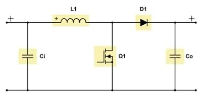
Figure 8: Non-synchronous boost converter schematic
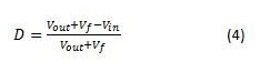
Equation 4 calculates the duty cycle:
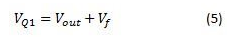
Equation 5 calculates maximum MOSFET stress:
Equation 6 gives the maximum diode stress:
Where Vin is the input voltage, Vout is the output voltage, and Vf is the diode forward voltage.
With a boost converter, you can see the pulsed output current because the LC filter is at the input. Therefore, the input current is continuous and the output voltage ripple is larger than the input voltage ripple.
When designing a boost converter, it is important to know that even when the converter is not switching, there is a permanent connection from the input to the output. Precautions must be taken to protect against possible short circuit events at the output.
For output currents greater than 4A, a synchronous rectifier should be used to replace the diode. If the power supply needs to provide an output current greater than 10A, it is strongly recommended to use multi-phase or interleaved power stages.
When operating in CCM mode, the dynamics of the boost converter are limited due to the right half-plane zero (RHPZ) of its transfer function. Since RHPZ cannot compensate, the achievable bandwidth will typically be less than one-fifth to one-tenth the RHPZ frequency. See Equation 7:
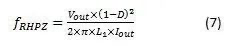
where Vout is the output voltage, D is the duty cycle, Iout is the output current, and L1 is the inductor of the boost converter.
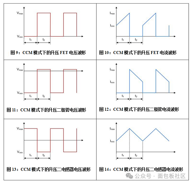
Figures 9 to 14 show the voltage and current waveforms of the FETs, diodes, and inductors in the nonsynchronous boost converter in CCM mode.
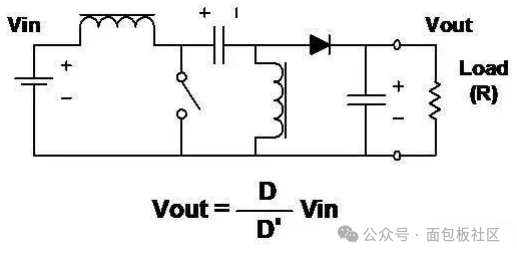
Buck-Boost Converter
A buck-boost converter is a combination of buck and boost power stages that share the same inductor. See Figure 15.
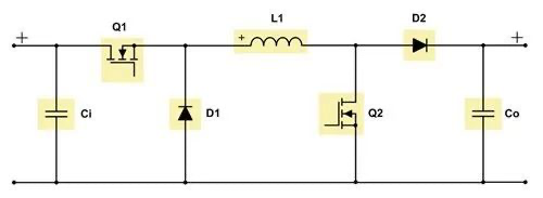
Figure 15: Dual-switch buck-boost converter schematic
The buck-boost topology is practical because the input voltage can be smaller, larger, or the same as the output voltage, requiring output power greater than 50W.
For output powers less than 50W, the single-ended primary inductor converter (SEPIC) is a more cost-effective option because it uses fewer components.
When the input voltage is greater than the output voltage, the buck-boost converter operates in buck mode; when the input voltage is less than the output voltage, it operates in boost mode. When the converter operates in the transmission region where the input voltage is within the output voltage range, there are two concepts for handling these situations: either the buck and boost stages are active simultaneously, or the switching cycles between the buck and boost stages. alternating, each typically operating at half the normal switching frequency. The second concept can induce sub-harmonic noise at the output and while the output voltage accuracy may not be as precise compared to regular buck or boost operation, the converter will be more efficient compared to the first concept.
The buck-boost topology has pulsating currents at both the input and the output because there are no LC filters in either direction.
For a buck-boost converter, the buck and boost power stage calculations can be used separately.
Buck-boost converters with two switches are suitable for power ranges between 50W and 100W (like the LM5118), with synchronous rectification up to 400W (same as the LM5175). It is recommended to use a synchronous rectifier with the same current limit as the uncombined buck and boost power stage.
You need to design the buck-boost converter’s compensation network for the boost stage because the RHPZ limits the regulator bandwidth.
Source: Texas Instruments
Supplement: Comparison of 20 switching power supply topologies
1. Common basic topologies:
■ Buck
■ Boost
■ Buck-Boost Buck-Boost
■ Flyback
■ Forward
■ Two-Transistor Forward
■ Push-Pull push-pull
■ Half Bridge Half Bridge
■ Full Bridge Full Bridge
■ SEPIC
■C’uk
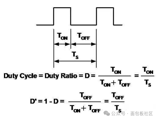
2. Basic pulse width modulation waveform
These topologies are related to switching circuits. The basic pulse width modulation waveform is defined as follows:
3. Buck reduces blood pressure
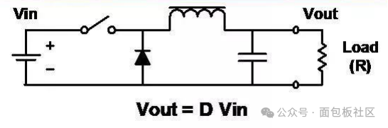
Features:
■ Reduce the input to a lower voltage
■ Possibly the simplest circuit
■ Inductor/capacitor filter flattens the square wave after switching
■ Output is always less than or equal to input
■ Input current is discontinuous (chopping)
■ Output current smoothing
4. Boost
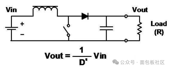
Features:
■ Boost the input to a higher voltage
■ Same as buck, but rearranged inductor, switch and diode
■ The output is always greater than or equal to the input (ignoring the forward voltage drop of the diode)
■ Input current smoothing
■ Output current is discontinuous (chopping)
5. Buck-Boost
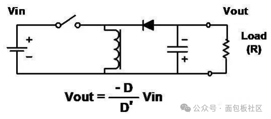
Features:
■Another arrangement of inductors, switches and diodes
■ Combines the disadvantages of buck and boost circuits
■ Input current is discontinuous (chopping)
■ The output current is also not continuous (chopping)
■ The output is always opposite to the input (note the polarity of the capacitor), but the amplitude can be smaller or larger than the input
■ A “flyback” converter is actually an isolated (transformer coupled) form of a buck-boost circuit.
6. Flyback
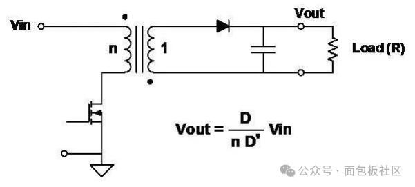
Features:
■ Works like a buck-boost circuit, but the inductor has two windings, acting as both a transformer and an inductor
■ The output can be positive or negative, determined by the polarity of the coil and diode.
■ The output voltage can be greater or less than the input voltage, determined by the turns ratio of the transformer.
■ This is the simplest of the isolation topologies
■ Multiple outputs can be obtained by adding secondary windings and circuits
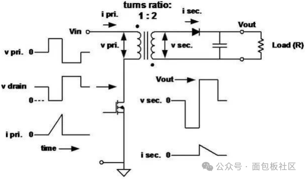
7. Forward
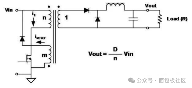
Features:
■ Transformer coupling form of step-down circuit.
■ Discontinuous input current, smooth output current.
■ Because of the transformer, the output can be larger or smaller than the input, and can be of any polarity.
■ Multiple outputs can be obtained by adding secondary windings and circuits.
■ The transformer core must be demagnetized during each switching cycle. A common practice is to add a winding with the same number of turns as the primary winding.
■ The energy stored in the primary inductance during the switch-on phase is released through the additional winding and diode during the switch-off phase.
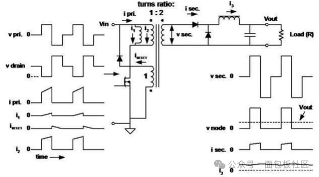
8. Two-Transistor Forward
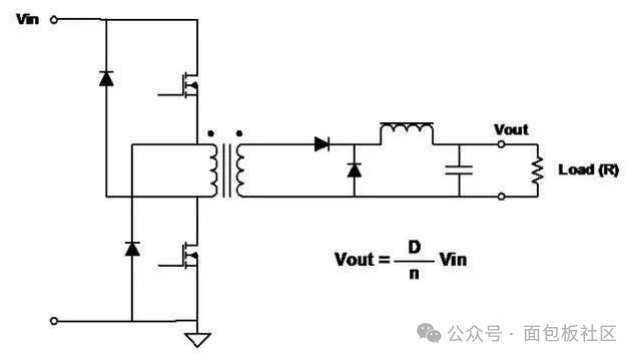
Features:
■ Both switches work simultaneously.
■ When the switch opens, the energy stored in the transformer reverses the polarity of the primary, causing the diode to conduct.
The main advantage:
■ The voltage across each switch never exceeds the input voltage.
■ No need to reset the winding track.
9. Push-Pull
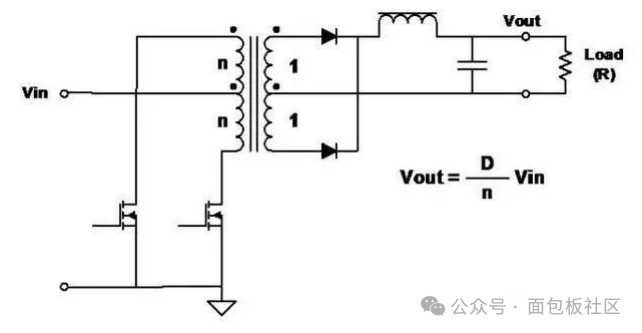
Features:
■ The switch (FET) is driven out of phase and pulse width modulation (PWM) is performed to regulate the output voltage.
■ Good transformer core utilization—power is transferred in both half-cycles.
■ Full-wave topology, so the output ripple frequency is twice the transformer frequency.
■ The voltage applied to the FET is twice the input voltage.
10. Half-Bridge
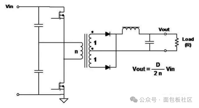
Features:
■ Very common topology for higher power converters.
■ The switch (FET) is driven out of phase and pulse width modulation (PWM) is performed to regulate the output voltage.
■ Good transformer core utilization—power is transferred in both half-cycles. Moreover, the utilization rate of the primary winding is better than that of the push-pull circuit.
■ Full-wave topology, so the output ripple frequency is twice the transformer frequency.
■ The voltage applied to the FET is equal to the input voltage.
11. Full-Bridge
Features:
■ Most common topology for higher power converters.
■ The switches (FETs) are driven in diagonal pairs and pulse width modulated (PWM) to regulate the output voltage.
■ Good transformer core utilization—power is transferred in both half-cycles.
■ Full-wave topology, so the output ripple frequency is twice the transformer frequency.
■ The voltage applied to the FETs is equal to the input voltage.
■ At a given power, the primary current is half that of a half-bridge.
12. SEPIC single-ended primary inductor converter
Features:
■ The output voltage can be greater or less than the input voltage.
■ Like the boost circuit, the input current is smooth, but the output current is discontinuous.
■ Energy is transferred from input to output through capacitance.
■ Two inductors are required.
13. C’uk (Slobodan C’uk’s patent)
Features:
■ Output inversion
■ The amplitude of the output voltage can be greater or less than the input.
■ Both input and output currents are smooth.
■ Energy is transferred from input to output through capacitance.
■ Two inductors are required.
■ Inductors can be coupled to obtain zero ripple inductor current.
14. Details of circuit operation
The following explains the working details of several topologies:
■ Buck regulator: continuous conduction, critical conduction, discontinuous conduction
■ Boost regulator (continuous conduction)
■ Transformer operation
■ Flyback transformer
■ Forward transformer
15. Buck-step-down regulator-continuous conduction
Features:
■ Inductor current is continuous.
■ Vout is the average value of its input voltage (V1).
■ The output voltage is the input voltage multiplied by the duty ratio of the switch (D).
■ When turned on, inductor current flows from the battery.
■ Current flows through the diode when the switch is open.
■ Neglecting losses in the switch and inductor, D is independent of load current.
■ The characteristics of buck regulators and their derivative circuits are:
The input current is discontinuous (chopping), and the output current is continuous (smoothing).
16. Buck-step-down regulator-critical conductivity
■ The inductor current is still continuous but “reaches” zero when the switch is turned on again. This is called “critical conduction.” The output voltage is still equal to the input voltage times D.
17. Buck-step-down regulator-discontinuous conduction
■ In this case, the current in the inductor is zero for a portion of each cycle.
■ The output voltage is still (always) the average value of v1.
■ The output voltage is not the input voltage times the duty ratio of the switch (D).
■ When the load current is below the critical value, D changes with the load current (while Vout remains constant).
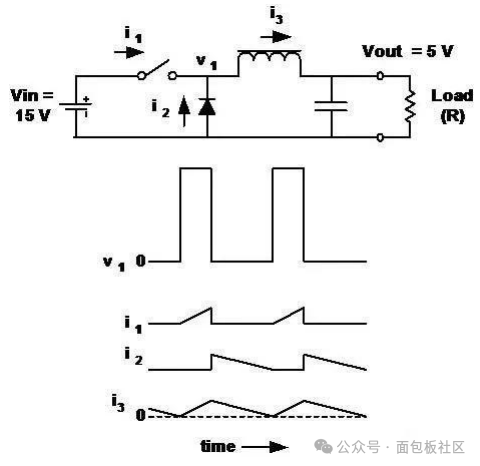
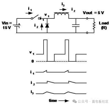
18. Boost boost regulator
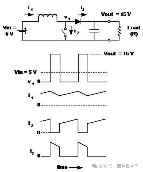
■ The output voltage is always greater than (or equal to) the input voltage.
■ Input current is continuous, output current is discontinuous (as opposed to a buck regulator).
■ The relationship between output voltage and duty ratio (D) is not as simple as in a buck regulator. In the case of continuous conduction:
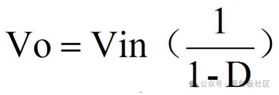
In this example, Vin = 5, Vout = 15, and D = 2/3. Vout = 15, D = 2/3.
19. Transformer operation (including the role of primary inductance)
■ The transformer is considered an ideal transformer with its primary (magnetizing) inductance connected in parallel with the primary.
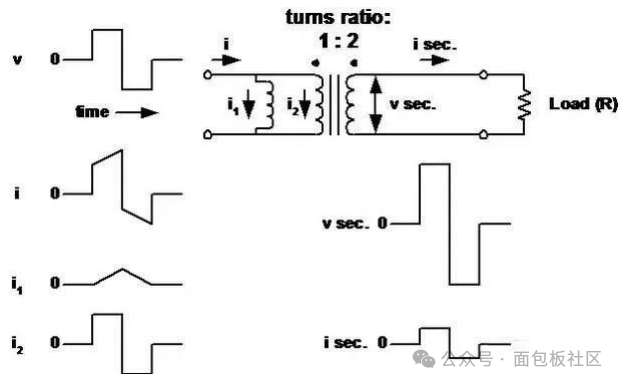
20. Flyback transformer
■ Here the primary inductance is low and is used to determine the peak current and stored energy. When the primary switch opens, energy is transferred to the secondary.
21. Forward conversion transformer
■ Primary inductance is high because there is no need to store energy.
■ The magnetizing current (i1) flows into the “magnetizing inductor”, causing the core to demagnetize (voltage reverse direction) after the primary switch opens.
22. Summary
■ The most common circuit topologies currently used in switching power supply conversion are reviewed here.
■ There are many more topologies, but mostly combinations or variations of the topologies described here.
■ Each topology involves unique design tradeoffs:
1) The voltage applied to the switch
2) Chopping and smoothing input and output current
3) Winding utilization
■ Choosing the best topology requires research on:
1) Input and output voltage range
2) Current range
3) Cost to performance, size to weight ratio