Table of Contents
Evaluate design metrics
1. Input parameters: input voltage size, AC or DC, number of phases, frequency, etc.
International voltage levels include single-phase 120Vac, 220Vac, 230Vac, etc. The internationally accepted AC voltage range is 85~265V. Generally includes the input voltage rating and its variation range;
Single-phase input is often used for power below 3kW, and three-phase input is used for power above 5kW;
Industrial power frequency is generally 50Hz or 60Hz, aerospace power supply and ship power frequency are 400Hz.
Whether there are power factor (Power Factor) and harmonics (Total Harmonics Distortion) indicators
2. Output parameters: output power, output voltage, output current, ripple, voltage stabilization (steady current) accuracy, adjustment rate, dynamic characteristics (settling time: settling time), power supply start-up time and holding time.
Output voltage: rated value + adjustment range. The upper limit of the output voltage should be as close as possible to the rated value to avoid unnecessary excessive design margin.
Output current: rated value + overload multiple. If there is a steady flow requirement, the adjustment range will also be specified. Some power supplies do not allow no load, so a lower current limit should also be specified.
Voltage and current stabilization accuracy: influencing factors include input voltage regulation rate, load regulation rate, and aging deviation. The accuracy of the reference source, the accuracy of the detection components, and the accuracy of the operational amplifier in the control circuit have a great influence on the accuracy of voltage stabilization and current stabilization.
3. Efficiency: the ratio of output power to input active power at rated input voltage, rated output voltage, and rated output current.
Losses: Losses closely related to switching frequency: switching losses of switching devices, iron losses of magnetic components, losses of absorption circuits.
Pass-state loss in the circuit: pass-state loss of switching devices, copper loss of magnetic components, line loss. This loss depends on the current.
Other losses: control circuit losses, drive circuit losses, etc. Generally, the efficiency of a power supply with a higher output voltage is higher than that of a power supply with a lower output voltage. The power supply efficiency of high output voltage can reach 90% to 95% efficiency. The efficiency of high-power circuits can be made higher than that of low-power circuits.
4. Voltage regulation rate and load regulation rate
Voltage (source) regulation rate: Power supply regulation rate is usually based on the deviation rate of the output voltage caused by changes in the input voltage under rated load conditions. As shown in the following formula: Vo(max)-Vo(min) / Vo(normal), or the deviation of the output voltage must be within the specified upper and lower limits, that is, within the absolute value of the upper and lower limits of the output voltage.
Load regulation: The definition of load regulation is the ability of a switching power supply to provide stable output voltage when the output load current changes. Or when the output load current changes, the output voltage deviation shall not exceed the upper and lower absolute values.
Test method: After the power supply under test stabilizes the heat engine under normal input voltage and load conditions, measure the output voltage value under normal load, and then measure the output voltage value under light load (Min) and heavy load (Max) respectively (respectively Vmax and Vmin), the load regulation rate is usually the percentage of the output voltage deviation rate caused by changes in load current under a normal fixed input voltage, as shown in the following formula: V0(max)-V0(min) / V0(normal)
5. Dynamic characteristics: changes in output voltage when load changes suddenly
The switching power supply ensures the stability of its output voltage through a feedback control loop. In fact, the feedback control loop has a certain bandwidth, which limits the response of the power supply to changes in load current, which may cause the switching power supply to become unstable, out of control, or oscillate. In fact, the load current of the power supply changes dynamically when it is working, so dynamic load testing is extremely important for the power supply.
Programmable electronic loads can be used to simulate the worst load conditions when the power supply is actually working, such as the rapid rise and fall of the load current, the slope, and the cycle. If the power supply is under severe load conditions, it can still maintain a stable output voltage. Do not cause overshoot or undershoot, otherwise the power supply output voltage will exceed the load component (for example, the output instantaneous voltage of a TTL circuit should be between 4.75V and 5.25V, so as not to cause the TTL logic circuit to malfunction) working range.
6. Power start-up time (Set-Up Time) and hold-up time (Hold-Up Time)
Start-up time: refers to the time from when the power supply is connected to the input until its output voltage rises to the regulated range. Taking a power supply with an output of 5V as an example, the startup time is from the time the power supply is turned on until the output voltage reaches 4.75V. until the time.
Holding time: The time from when the input power is cut off until the output voltage drops outside the regulated range. Taking a power supply with an output of 5V as an example, the holding time is from the time the power is turned off until the output voltage is lower than 4.75V. Time, the general value is 10-20ms, to avoid the load operation being affected due to short-term voltage interruption (half or one grid voltage cycle) in the power supply of the power company.
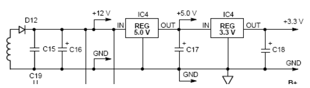
7. Cross adjustment rate of multi-channel output power supply:
Multi-output also needs to consider the cross adjustment rate (Cross Regulation).
What is the cross adjustment rate?
When the load of one output changes, the range of change of the other output voltage.
Conventional methods to improve cross-adjustment rate: post-stage adjustment
Such as: low power multi-channel output Flyback
Input voltage range…………90~264VAC, 120-370VDC
Input current………………….2.0A/115V 1.1A/230V, input frequency: 47~63HZ
Inrush current…………. Cold starting current 20A/115V 40A/230V
Leakage current…………….< 2mA/240VAC
Output voltage adjustment range……….CH1: -5~+10%
Voltage regulation rate…………CH1: < 1%, CH2: < 1%
Load regulation rate……CH1: < 3%, CH2/3: < 4-8%
Overload protection…………105%~150% Protection type: current limit, automatic recovery
Overvoltage protection…………115-135%CH1 rated output voltage
Temperature coefficient…………±0.03%℃(0~50℃)
Start, rise, hold time…800ms, 60ms, 20ms
Shock resistance…………10~500Hz, 2G, three axes 10min./1 cycle, 1 hour per axis
Pressure resistance………………….Input-output: 3KVAC, input-casing: 1.5KVAC,
Output-Enclosure: 0.5KVAC 1 minute
Insulation resistance…………Input-output, input-ground, output-ground 500VDC/100M Ohms
Working temperature and humidity……-10℃~+60℃, 20%~90%RH (0-45℃/100%, -10℃/80%, 60℃/60 % LOAD)
Storage temperature and humidity……-20℃~+85℃, 10%~95RH
Overall dimensions…………199*99*50mm CASE 916A
Weight…………0.6kg; 20pcs/13kg/1.17CUFT
Safety standards………………….Meet UL1310, TUV EN60950 requirements
EMC/Harmonic Standards…………Meet
EN55022 class B/A,EN61000-3-2,3
EN61000-4-2,3,4,5,6,8,11,ENV50204
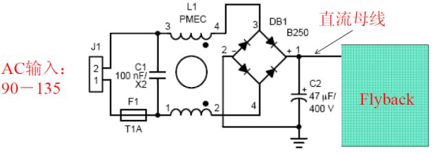
2. Select the appropriate main circuit topology (AC-DC)
Basic principles: power level, cost, efficiency, size
When the power is below 75 watts, there is generally no restriction on input side harmonics. Therefore, a flyback circuit with simple circuit and low cost is selected. Japan limits power below 50W. The lighting requirement is higher, 25W.
The general power supply requirements for circuit power above 75 watts meet the harmonic IEC61000-3-2. Power factor correction is generally required, so a two-stage solution is mostly used. Boost PFC+Flyback; <100W, Boost PFC+half bridge 100W< <500W
For higher power (above 500 watts), half-bridge or full-bridge can be used. If cost requirements are strict, choose half-bridge, and if power is high, choose full-bridge. Push-pull circuits are usually used in situations where the power is relatively high and the input voltage is very low.
Generally, when the power is less than 20W, since the losses of the power supply are mainly magnetic components, switches, and drive losses, the proportion of on-state losses is small (the current is small), so a solution with a simple circuit topology is chosen. Such as DCM Flyback.
When the loss of the power supply is mainly pass-state loss (high power, or low voltage and high current), it is necessary to consider a solution that can reduce pass-state loss. For example: synchronous rectification, multi-stage conversion, parallel connection, hybrid topology, etc.
3. Component design
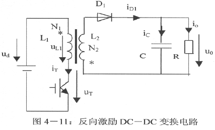
Example: Which components in the main circuit of Flyback need to be designed by us?
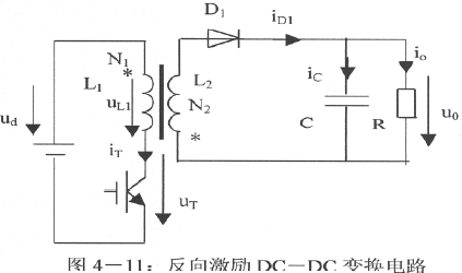
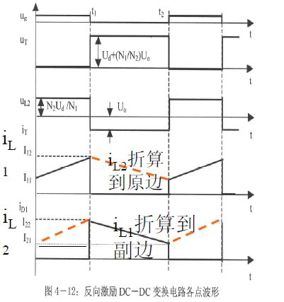
① Calculate the circuit operating parameters. Input and output voltage
② Operating parameters. Switching frequency, maximum duty cycle
③ Transformer.
④ Switch tube – voltage, current
⑤ Secondary side diode – voltage, current
⑥ Output filter capacitor
⑦ Absorption circuit
design steps
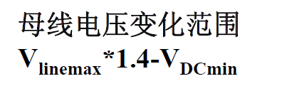
(1) Determine the voltage variation range of the input DC bus:
1) Range changes with input
2) Voltage changes within each power frequency cycle
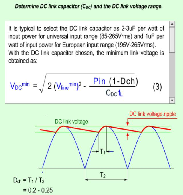
(2) Design switching frequency fs, maximum duty cycle Dmax=0.45
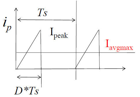
• Set switching frequency as required
• Based on the input power, and assuming the lowest voltage and maximum duty cycle, just critical continuity, then determine the inductor peak current
Pinmax=Pomax/efficiency
Iavgmax=Pinmax/VDCmin
Ipeak=2*Iavgmax/D
(3) Design flyback transformer
– Determine the primary inductance based on the maximum peak current
Pinmax=0.5*Lm*Ipeak2*fs
– Based on experience, select the core size and calculate the number of primary turns.
Np=(Lm*Ipeak)/(Ae*Bmax)
Ae is the core cross-sectional area; Bmax is the designed maximum magnetic flux density.
– Design the air gap based on the inductance and number of turns.
– Select the appropriate turns ratio based on the rated voltage of the primary switch. In order to obtain better secondary cross regulation, it is sometimes necessary to adjust the number of turns on the primary side of the transformer.
Example: secondary side Vo1: Vo2=5:3
Preliminary calculations show: Ns1=3, Ns2=1.8; if Ns2 takes 2 turns, the adjustment rate may be poor. Therefore, modify the number of secondary turns, Ns1=5, Ns2=3.
(4) Switch tube selection: power MOSFET
Switch voltage stress:
For example: If a 650V MOSFET is selected on the primary side, the voltage stress of the switch tube on the primary side should not exceed 600V.
So calculate the maximum stress: Vpmax=VDCmax+(Vo+Vdrop)*Np/Ns+60V
Switch tube current stress:
Calculate the maximum current on the primary side of the transformer
Normally: Vo*Np/Ns<140V;
Consider a compromise between the stress of the primary switch tube, the voltage stress of the secondary diode, and the maximum duty cycle.
(5) Selection of secondary side diode:
– Fast recovery diode
– Calculate the withstand voltage of the diode
VD=(Vdcmax*Ns/Np+Vo)*1.3
(6) Selection of output filter capacitor:
Select electrolytic capacitors based on current/voltage stress, ripple requirements.
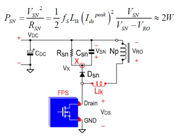
(7) RCD absorption circuit
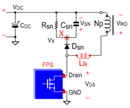
Consider the problem points:
1) Absorption effect
2) The loss is likely to be small
Compromise between absorption effect and loss!
The same design principle applies not only to FLYback, but also to all absorption circuits with R.
Loss estimation method:
1) Psnuber=Vc2/R
When the MOSFET is turned off, when Vds exceeds the voltage VSN across the capacitor in the RCD snubber circuit, the snubber diode is turned on. The peak current is absorbed by the RCD circuit, thereby reducing the peak current. The snubber capacitor must be large enough to ensure that a switch The voltage across the capacitor does not change significantly during the cycle. However, if the absorption capacitance is too large, it will also increase the loss of the buffer circuit. There must be a compromise.
The power consumed by the absorption circuit can be calculated by the following formula. Then take a power resistor with a resistance of 3W, and its resistance and capacitance values can be calculated by the software, as shown below
4. Other modes of flyback design
CCM/DCM Flyback design
When the power is larger, such as 65W. In order to reduce low pressure
The conduction loss at input causes the device to enter CCM mode at low voltage input. When high voltage is input, DCM mode.
The design steps are the same as the DCM model, but the design formula is different.
– The formula for calculating the primary inductance value is different
– The formula for calculating turns ratio is different
– Calculate the different voltage and current stress of switch tubes
– Calculate diode voltage and current stress differences
– Calculated output ripple is different Boundary CM Flyback
Within the varying range of bus voltage, the mode is critical. (Frequency conversion) The same steps and method patterns as DCM design.
BCM/DCM advantages:
1) The turn-on loss of the primary switch tube is small.
2) The reverse recovery current of the secondary side diode is small.
3) The common mode noise caused by reverse recovery is small
4) The voltage stress of the diode is small, so low-voltage devices should be selected.
Disadvantages of BCM model:
1) The conduction loss of the primary switch tube is large.
2) Frequency changes, the differential mode filter needs to be designed according to the lowest frequency. Common mode filters should be designed for higher frequencies.
Two conditions make the above shortcomings no longer important:
1) With the improvement of MOSFET devices, Rdson is getting smaller and smaller. Reduce the proportion of the primary conduction loss to the total loss.
2) BCM reduces the common mode caused by the reverse recovery of the diode on the secondary side.
5. Thermal design
The switch tube generally needs a radiator, and an insulating gasket and heat-dissipating silicone should be applied between the radiator and the switch tube.
In the design of high-power switching power supplies, fans are generally installed to use forced air cooling.
6. Wiring design and EMI
The pins of each component, especially the capacitor, should be as short as possible, otherwise the capacitor will have poor absorption effect on high frequencies;
Interconnecting wires through which large currents flow should be thick or short;
Try not to form a large loop, otherwise the interference will be too great and affect debugging.
The control circuit wiring should be separated from the power circuit wiring.
The control chip and transformer must be installed with seats to facilitate disassembly. When wiring, give full consideration to heat dissipation and convenience for testing. It is neat and tidy, and each functional module is clear.